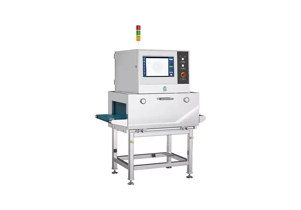
 X-ray for food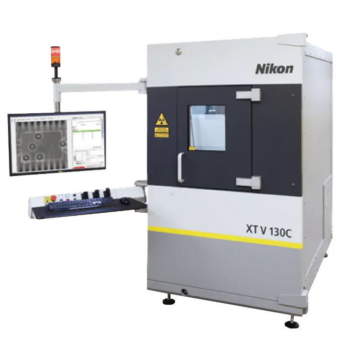
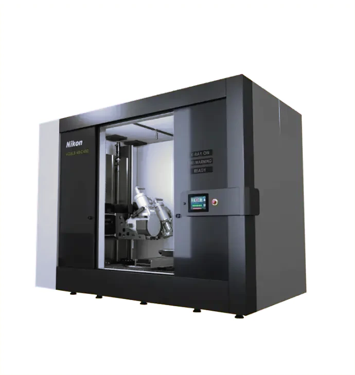
Nikon
XT V 130C
Compact microfocus X-ray for PCB, BGA, connectors and small electronic components.
130 kVManual inspection
ELECTRONICS X-RAY INSPECTION
2D, 2.5D and CT inspection for PCB, BGA, semiconductors, connectors and electronic assemblies — from lab to SMT line.
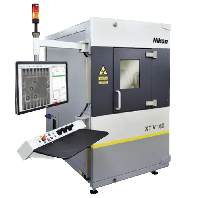
X-RAY AND CT ECOSYSTEM
Navigate by technology and compare solutions for your application.
X-RAY RANGE FOR ELECTRONICS
Nikon and Unicomp solutions for solder defects, voids, misaligned components, BGA, chips and reel counting.
Compact microfocus X-ray for PCB, BGA, connectors and small electronic components.
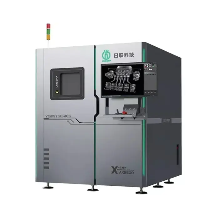
Premium 2D and CT inspection for electronics, semiconductors and complex devices.
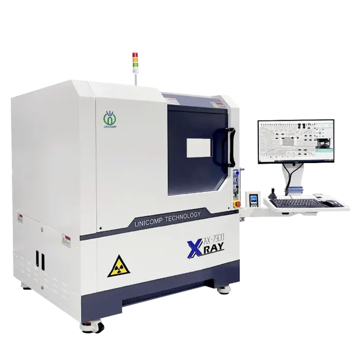
Compact system for PCB, BGA, LED and small assembly inspection.
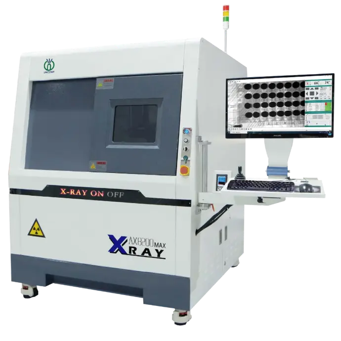
High resolution for solder joints, voids, BGA and electronic-component inspection.
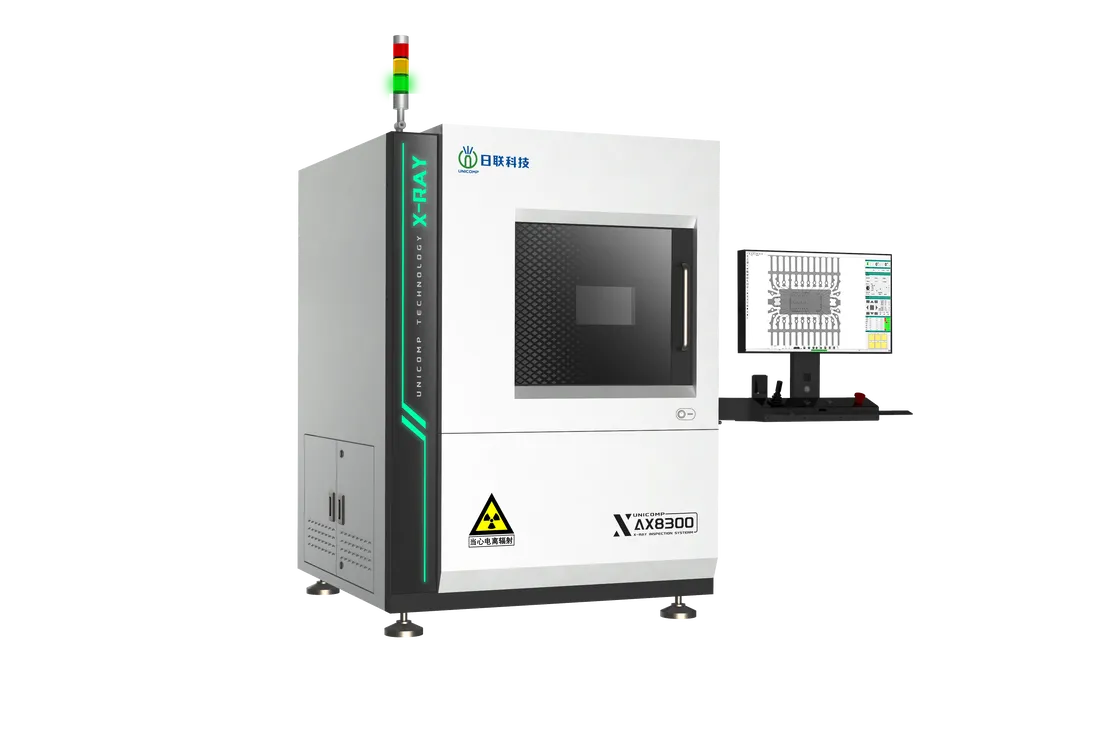
High-magnification platform for detailed PCBA and semiconductor inspection.
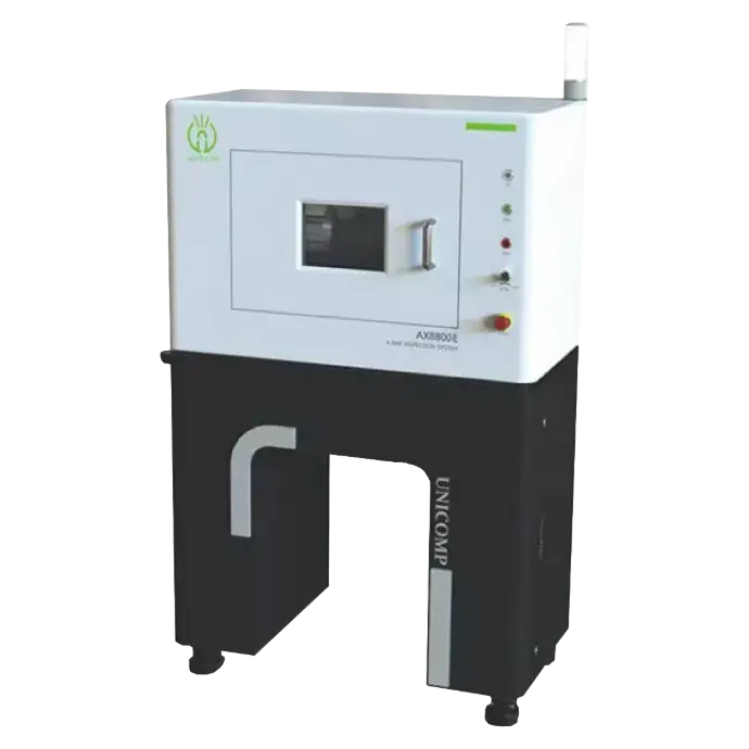
Advanced inspection with flexible manipulation for larger samples and assemblies.
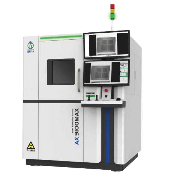
Family for high resolution, high magnification and demanding defect inspection.
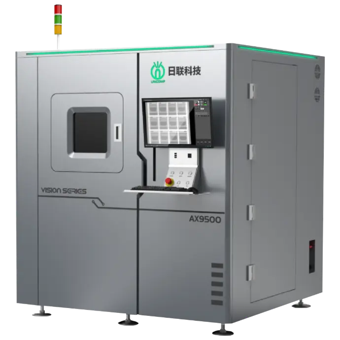
Inspection for larger boards and assemblies with precise positioning.
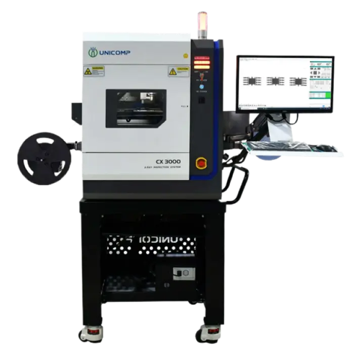
Automatic X-ray counting of reel components for logistics and SMT.
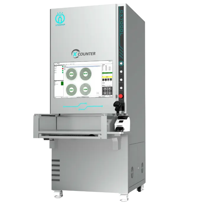
Intelligent multi-reel counting for electronics warehousing and production.
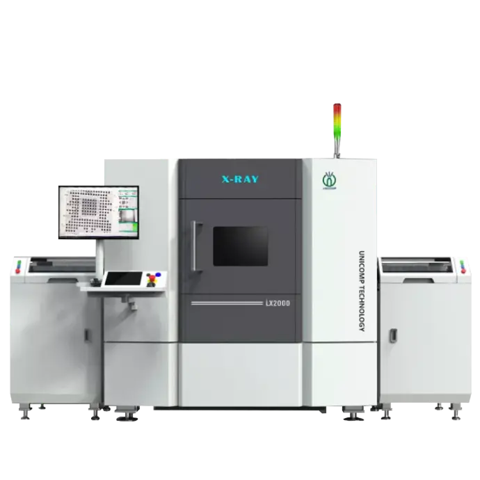
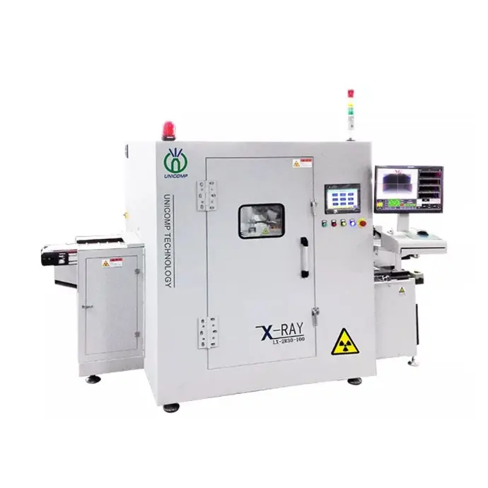
Inline X-ray inspection for automated production component control.
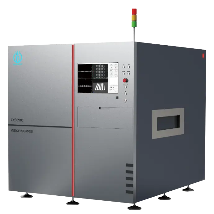
High-throughput automated inspection for SMT lines and process control.
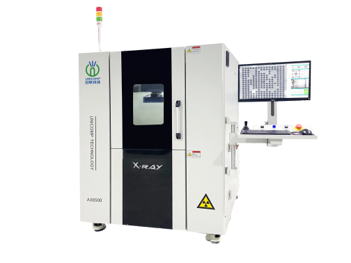
110 kV X-ray for leadframes, semiconductors, power electronics and high-precision inspection.
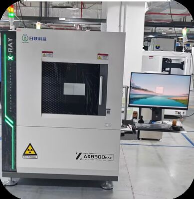
Inspection of MOSFET, ceramics, BGA and PCBA with advanced void and crack visualisation.
FROM IMAGE TO DECISION
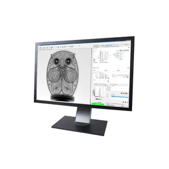
Automated BGA, wire-bond, PTH and PoP measurement with pass/fail decisions.
Keep the region of interest in view even at high magnification.
Reveal high- and low-contrast detail simultaneously.
Collision avoidance, low dose and ESD options for sensitive devices.
APPLICATION-LED SELECTION
Send us the part, the defect you need to detect and the inspection rate. NM3D will recommend the right technology, source, detector and software.
Request a recommendationSend us a board or component and the target defect so we can define the most effective configuration.
Request a demo or quote